Niobium nitride
 | |
| Names | |
|---|---|
| IUPAC name
Niobium nitride
| |
| Identifiers | |
CAS Number
|
|
3D model (JSmol)
|
|
| ChemSpider | |
| ECHA InfoCard | 100.042.132 |
| EC Number |
|
PubChem CID
|
|
InChI
| |
SMILES
| |
| Properties | |
Chemical formula
|
NbN |
| Molar mass | 106.91 g/mol |
| Appearance | gray solid |
| Density | 8.470 g/cm3 |
| Melting point | 2,573 °C (4,663 °F; 2,846 K) |
Solubility in water
|
reacts to form ammonia |
| Structure | |
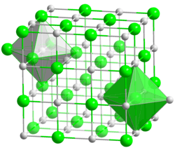
Crystal structure
|
cubic, cF8 |
Space group
|
Fm3m, No. 225 |
| Hazards | |
| Flash point | Non-flammable |
| Safety data sheet (SDS) | External MSDS |
| Related compounds | |
Other cations
|
Vanadium nitride Tantalum nitride |
Except where otherwise noted, data are given for materials in their standard state (at 25 °C [77 °F], 100 kPa).
Infobox references
| |
Niobium nitride is a chemical compound of niobium (element 41) and nitrogen (element 7) with the chemical formula NbxNy. At room temperature it is metallic with sputtered films showing a moderate conductivity of 12.2 to 14.3 μΩ cm.[1] It is also very hard having a vickers hardness of around 20 GPa.[2] At low temperatures (~16 K) NbN becomes a superconductor; this property is widely used in precise detectors for infrared light and is being investigated for superconducting resonators.[3]
History and use
Niobium nitride (NbN) was first identified during early crystallographic studies of transition-metal nitrides in the 1940s, with the δ-NbN structure resolved by x-ray diffraction (Aschermann et al 1941). At the time of its discovery it was notable for having the record high superconducting transition temperature (TC).[4] Improvements in reactive sputtering enabled high-quality NbN films for superconducting electronics. In the early 2000s, NbN became the foundational material for superconducting nanowire single-photon detectors (SNSPDs), owing to its high Tc and robust nanometer-scale fabrication.[5] Since then, NbN-based SNSPDs have demonstrated single-photon sensitivity across the 1–10 μm infrared range [6]—important for astronomy, quantum communications, and telecommunications—and can operate at count rates up to 25 GHz.2 NbTiN nanowires are the state of the art technology for SNSPDs achieving near unity detection efficiency and timing resolution below 3 pm.[7]
Beyond superconducting devices, niobium nitride is employed in a variety of optical and materials-engineering roles. NbN thin films serve as absorbing or anti-reflective coatings, taking advantage of their tunable optical constants. In 2015, Panasonic reported a photocatalyst based on niobium nitride capable of absorbing approximately 57% of sunlight to drive water-splitting reactions for hydrogen production.[8] Today, NbN remains widely used in superconducting electronics, quantum photonics, and refractory surface coatings.
Properties
Physical
NbN is generally considered to be a very stable material meaning it resists corrosion or oxidation. However, as mentioned above, it is primarily used for superconducting quantum devices. This means even very slight penetration of chemicals into its surface can harm device properties significantly. This is a topic of ongoing research.[9] As mentioned above, it also has moderately high hardness of 20 GPa, but TiN still dominates coating technologies due to better thermal stability.[10]
Electrical
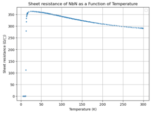
The electrical properties of niobium nitride vary significantly depending on deposition method, film thickness, and substrate choice, as these factors strongly influence disorder and carrier concentration. A representative experiment may be sputtered NbN grown epitaxially on MgO (100), typical values fall within a broad but well-established range. Hall and magnetotransport measurements show that the normal-state resistivity can range from approximately 0.9–3.8 μΩ·m and that the superconducting transition temperature correspondingly varies from ~10 K to ~16 K. The carrier density is highly sensitive to stoichiometry and nitrogen content, increasing by roughly a factor of three between low-Tc, high-resistivity films and high-Tc, low-resistivity films, whereas the carrier mobility remains comparatively unchanged.[11] By tuning nitrogen concentration during sputtering, the effective disorder level (quantified by the product ) can be varied from the moderately clean limit to the dirty limit, making NbN a useful platform for studying the interplay of carrier density, disorder, and superconductivity in an s-wave system.

Niobium nitride is a type-II superconductor with a critical temperature in the range of 16–18 K. According to data reported in ASM Handbook, Volume 2, NbN exhibits a thermodynamic critical field of approximately μ0Hc ≈ 0.16 T, with lower and upper critical fields of μ0Hc1 ≈ 0.004 T and μ0Hc2 between 20–35 T, respectively. The material has a magnetic penetration depth of roughly 600 nm and a coherence length near 5 nm, reflecting its type-II character. NbN also supports high critical current densities, with reported values around 10 kA·mm−2 (at 0 T).[10]
Phases and crystallography
Niobium nitride (NbNx) exhibits a rich variety of crystallographic phases depending on nitrogen content x, temperature, and synthesis method. The structural and physical properties of these phases have been extensively reviewed in the literature.[13] NbNx can be prepared as powders, diffusion couples, and most commonly thin films.[14]
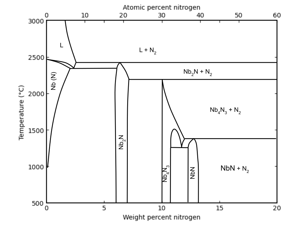
The Nb–N binary phase diagram (shown right) illustrates the equilibrium stability fields of phases such as Nb2N, Nb4N3, and NbNx, though it does not include metastable phases or thin-film effects. In practice, the metastable cubic δ-NbN remains the technologically dominant phase due to its superconducting properties, ease of growth in sputtering and MBE systems, and structural compatibility with commonly used substrates.
Experimental studies of the Nb–N system identify several nitrogen-rich phases, each with distinct structures and stability ranges.[12] The phases are tabulated in the following table:
| Phase Formula | Composition (wt% N) | Pearson Symbol | Space Group | Notes |
|---|---|---|---|---|
| Nb (solid solution) | 0 to <3 | cI2 | Im3m | bcc Nb with small N solubility |
| Nb2N | ~5.9 to 7 | hP9 | P31m | Hexagonal subnitride |
| Nb4N3 | ~10.2 | tI14 | I4/mmm | Tetragonal defect nitride |
| NbN | ~13.1 | cF8 | Fm3m | Cubic rocksalt NbN; metastable at room temperature and pressure; common thin-film and superconducting phase |
| ~13.1–15 (N-rich) | hP8 | P63/mmc | Hexagonal ε-NbN; not superconducting |
An issue published in 2010 associates these intermetallic phases with specific stoichiometry ranges and details the transitions between them.[13]
- δ-NbNx (0.72 < x < 1.06) — a NaCl-type cubic structure (space group Fm3̄m) stable at high temperatures, typically above Ttransition = 1070–1225 °C. In this phase, nitrogen (or niobium in the case x > 1) vacancies are arranged statistically, meaning they have no long range order. This randomness maintains the highly symmetric cubic structure.
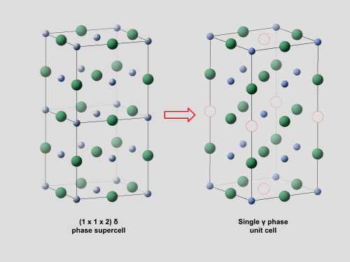
- γ-Nb4N3 also written γ-NbNx (0.72 < x < 0.84) — a body-centered tetragonal structure (space group I4/mmm).5 This phase is stable below Ttransition and transforms into δ-NbNx above. It is known that the delta phase transforms into gamma by assembling a 1 x 1 x 2 supercell which has ordered vacancies as shown right. Despite this, the detailed mechanism of the δ → γ transformation remains unresolved.
- ε-NbNx (0.95 < x < 0.98) — a hexagonal phase described by an anti-WC-type structure (P6̄m2). ε-NbN is stable below 1330 °C.
- δ′-NbNx — a hexagonal variant with an anti-NiAs-type structure (P63/mmc). This phase is believed to form only transiently during the transformation of ε-NbN into δ-NbN.
Despite the large number of stable and metastable phases predicted in the Nb–N binary system, thin-film experiments overwhelmingly report the formation of the δ-NbN cubic phase. This is notable because δ-NbN is metastable at room temperature and pressure, its absence from the equilibrium Nb–N phase diagram and ab-initio calculations support this classification.[15] Nevertheless, thin-film deposition techniques often stabilize δ-NbN through non-equilibrium growth pathways, high nitrogen chemical potential, and large epitaxial or compressive stresses imposed by the substrate.[16] These factors shift the effective free-energy landscape, enabling δ-phase formation even in conditions where equilibrium thermodynamics would favor other phases such as ε-NbN or γ-Nb4N3.
Deposition techniques
Niobium nitride (NbN) is commonly deposited as a thin film for electronic, photonic, superconducting, and protective-coating applications. A wide range of physical and chemical vapor deposition methods are used, each offering different trade-offs in crystallinity, phase control, growth temperature, and equipment complexity. Major approaches include sputtering, molecular beam epitaxy (MBE), and chemical vapor deposition (CVD), along with more specialized processes such as atomic layer deposition (ALD) and thermal laser epitaxy (TLE).
Sputtering
Sputtering is the most widely accessible technique for NbN due to its relatively low cost and straightforward operation. In reactive sputtering, a niobium metal target is bombarded by nitrogen plasma, ejecting Nb atoms that react with nitrogen in the chamber or on the substrate surface to form NbN. This method commonly produces films in the δ-NbN (cubic) phase. While sputtering is robust and scalable, it offers limited control over stoichiometry, defect density, and crystallinity compared to epitaxial growth techniques. Film stress, grain size, and phase purity are sensitive to nitrogen flow rate, plasma power, and substrate temperature among other deposition parameters.[17]
Chemical vapor deposition
Chemical vapor deposition (CVD) routes, including thermal CVD, plasma-enhanced CVD, and metal-organic CVD (MOCVD), enable NbN growth from Nb-containing volatile precursors reacting with nitrogen sources such as NH3. These techniques can yield smoother films with improved uniformity and thickness control compared to sputtering. However, the requirement for specialized organometallic precursors and high-temperature processing increases equipment cost and operational complexity. CVD-grown NbN films can access multiple phases (δ, ε, or hexagonal variants) depending on precursor chemistry and growth parameters.
Molecular beam epitaxy
Molecular beam epitaxy (MBE) offers the highest level of control over film crystallinity and phase through ultra-high vacuum growth and atomic-scale flux tuning. In NbN MBE, a niobium source must be heated to extremely high temperatures to generate sufficient vapor pressure. Because Nb's melting point (2477 °C) exceeds the operating range of standard effusion cells, electron-beam evaporation is typically required. The evaporated Nb beam reacts with an activated nitrogen source, either a nitrogen plasma or ammonia, prior to incorporation at the substrate surface. Precise stoichiometry control is essential, as deviations in the Nb:N ratio strongly influence phase stability.[14]
Epitaxial NbN films have been successfully grown on substrates such as MgO, Si(100), sapphire (Al2O3), and GaN(0001). These substrates help stabilize the cubic δ-NbN phase through lattice matching and controlled interfacial strain. While MBE can produce highly crystalline films with low defect densities which is critical for superconducting and quantum device applications, the method is expensive, slow, and technically demanding.
Emerging and specialized methods
Techniques such as atomic layer deposition (ALD) and thermal laser epitaxy (TLE) offer additional options for NbN films. ALD enables extremely conformal coatings with sub-nanometer thickness control, making it attractive for nanoscale device architectures, though precursor availability remains limited. TLE uses a focused laser to evaporate a niobium target which is close to the substrate. This reduced path length allows for higher chamber pressures enabling even more control of the growth process. Further laser heating of the substrate means TLE can reach higher substrate temperatures making it a promising new processing method.
Characterization
Xray diffraction
| h | k | l | d (Å) | 2θ (°) | I (relative) |
|---|---|---|---|---|---|
| 1 | 1 | 1 | 2.53688 | 35.3527 | 100.0 |
| 2 | 0 | 0 | 2.19700 | 41.0496 | 85.3748 |
| 2 | 2 | 0 | 1.55351 | 59.4505 | 49.5187 |
| 3 | 1 | 1 | 1.32484 | 71.1018 | 34.2775 |
| 2 | 2 | 2 | 1.26844 | 74.7861 | 15.1564 |
| 4 | 0 | 0 | 1.09850 | 89.0509 | 6.9973 |
| 3 | 3 | 1 | 1.00805 | 99.6616 | 15.0928 |
| 4 | 2 | 0 | 0.98253 | 103.2550 | 22.0798 |
| 4 | 2 | 2 | 0.89692 | 118.3690 | 21.6595 |
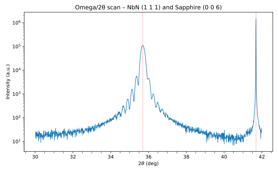
The above table presents powder diffraction data simulated in VESTA for cubic δ-NbN. It lists all allowed reflections for a randomly oriented crystallite ensemble. The ω–2θ scan shown right has a single strong NbN (111) peak at 35.7°, accompanied by clear thickness fringes. These fringes result from interference between X-rays reflected at the film surface and the film–substrate interface, and their visibility indicates a smooth, uniform, and well-defined epitaxial NbN layer. These fringes are characteristic of epitaxy.
Transmission electron microscopy
Transmission electron microscopy (TEM) is frequently used to examine the microstructure of NbN films and their interfaces. Multiple studies report that MBE-grown NbN transitions to columnar growth once the film exceeds a critical thickness of ~10 nm.[18][19] Critical thickness refers to the maximum film thickness at which an epitaxial layer can be maintained before strain relaxation occurs through defect formation or a change in growth mode. In NbN, surpassing this thickness leads to strain relaxation and the onset of columnar grains, which limits achievable crystallinity and presents challenges for fabricating high-performance quantum devices. Ongoing research continues to explore growth conditions and nitrogen chemistry to suppress or delay this transition.
References
- ^ Shoji, A.; Kiryu, S.; Kohjiro, S. (1992-03-30). "Superconducting properties and normal-state resistivity of single-crystal NbN films prepared by a reactive rf-magnetron sputtering method". Applied Physics Letters. 60 (13): 1624–1626. Bibcode:1992ApPhL..60.1624S. doi:10.1063/1.107220. ISSN 0003-6951.
- ^ Chen, Xiao-Jia; Struzhkin, Viktor V.; Wu, Zhigang; Somayazulu, Maddury; Qian, Jiang; Kung, Simon; Christensen, Axel Nørlund; Zhao, Yusheng; Cohen, Ronald E.; Mao, Ho-kwang; Hemley, Russell J. (March 2005). "Hard superconducting nitrides". Proceedings of the National Academy of Sciences. 102 (9): 3198–3201. Bibcode:2005PNAS..102.3198C. doi:10.1073/pnas.0500174102. PMC 552926. PMID 15728352.
- ^ Frasca, S.; Arabadzhiev, I.N.; de Puechredon, S.Y. Bros; Oppliger, F.; Jouanny, V.; Musio, R.; Scigliuzzo, M.; Minganti, F.; Scarlino, P.; Charbon, E. (2023-10-09). "NbN films with high kinetic inductance for high-quality compact superconducting resonators". Physical Review Applied. 20 (4) 044021. arXiv:2302.13930. Bibcode:2023PhRvP..20d4021F. doi:10.1103/PhysRevApplied.20.044021. ISSN 2331-7019.
- ^ Blundell, Stephen (2009). Superconductivity: A Very Short Introduction. Oxford University Press. ISBN 978-0-19-954090-7.
- ^ Natarajan, Chandra M; Tanner, Michael G; Hadfield, Robert H (2012-04-04). "Superconducting nanowire single-photon detectors: physics and applications". Superconductor Science and Technology. 25 (6) 063001. arXiv:1204.5560. Bibcode:2012SuScT..25f3001N. doi:10.1088/0953-2048/25/6/063001. ISSN 0953-2048.
- ^ M Hajenius, J J A Baselmans, J R Gao, T M Klapwijk, P A J de Korte, B Voronov and G Gol'tsman (2004). "Low noise NbN superconducting hot electron bolometer mixers at 1.9 and 2.5 THz". Superconductor Science and Technology. 17 (5): S224–S228. Bibcode:2004SuScT..17S.224H. doi:10.1088/0953-2048/17/5/026. S2CID 250740737.
{{cite journal}}: CS1 maint: multiple names: authors list (link) - ^ Dong, Shuyu; Koh, Darren Ming Zhi; Martinelli, Filippo; Brosseau, Pierre J. E.; Petrović, Milos; Shen, Lijiong; Adamo, Giorgio; Vetlugin, Anton N.; Sidorova, Mariia; Kurtsiefer, Christian; Soci, Cesare (2024-12-28). "Establishing an end-to-end workflow for SNSPD fabrication and characterization". Scientific Reports. 14 (1): 30891. Bibcode:2024NatSR..1430891D. doi:10.1038/s41598-024-81776-2. ISSN 2045-2322. PMC 11680598. PMID 39730607.
- ^ Yamamura, Tetsushi (August 2, 2015). "Panasonic moves closer to home energy self-sufficiency with fuel cells". Asahi Shimbun. Archived from the original on August 7, 2015. Retrieved 2015-08-02.
- ^ Zheng, K.; Kowsari, D.; Thobaben, N. J.; Du, X.; Song, X.; Ran, S.; Henriksen, E. A.; Wisbey, D. S.; Murch, K. W. (2022-03-07). "Nitrogen plasma passivated niobium resonators for superconducting quantum circuits". Applied Physics Letters. 120 (10) 102601. arXiv:2201.01776. Bibcode:2022ApPhL.120j2601Z. doi:10.1063/5.0082755. ISSN 0003-6951.
- ^ a b ASM Handbook, Volume 2: Properties and Selection: Nonferrous Alloys and Special-Purpose Materials. Materials Park, OH: ASM International. 1990.
- ^ Chockalingam, S. P.; Chand, Madhavi; Jesudasan, John; Tripathi, Vikram; Raychaudhuri, Pratap (2008-06-04). "Superconducting properties and Hall effect of epitaxial NbN thin films". Physical Review B. 77 (21) 214503. arXiv:0804.2945. Bibcode:2008PhRvB..77u4503C. doi:10.1103/PhysRevB.77.214503. ISSN 1098-0121.
- ^ a b ASM International (1992). ASM Handbook, Volume 3: Alloy Phase Diagrams. Materials Park, OH: ASM International. ISBN 0-87170-377-7.
- ^ a b Ivashchenko, V. I.; P. E. A. Turchi; Olifan, E. I. (2010-08-13). "Phase stability and mechanical properties of niobium nitrides". Physical Review B. 82 (5) 054109. Bibcode:2010PhRvB..82e4109I. doi:10.1103/PhysRevB.82.054109. Archived from the original on 2025-07-09. Retrieved 2025-12-11.
- ^ a b Iovan, A.; Pedeches, A.; Descamps, T.; Rotella, H.; Florea, I.; Semond, F.; Zwiller, V. (2023-12-18). "NbN thin films grown on silicon by molecular beam epitaxy for superconducting detectors". Applied Physics Letters. 123 (25) 252602. Bibcode:2023ApPhL.123y2602I. doi:10.1063/5.0175699. ISSN 0003-6951.
- ^ Isaev, E. I.; Simak, S. I.; Abrikosov, I. A.; Ahuja, R.; Vekilov, Yu. Kh.; Katsnelson, M. I.; Lichtenstein, A. I.; Johansson, B. (2007-06-15). "Phonon related properties of transition metals, their carbides, and nitrides: A first-principles study". Journal of Applied Physics. 101 (12) 123519. Bibcode:2007JAP...101l3519I. doi:10.1063/1.2747230. ISSN 0021-8979. Archived from the original on 2023-05-12. Retrieved 2025-12-11.
- ^ Koch, R (1994-11-07). "The intrinsic stress of polycrystalline and epitaxial thin metal films". Journal of Physics: Condensed Matter. 6 (45): 9519–9550. Bibcode:1994JPCM....6.9519K. doi:10.1088/0953-8984/6/45/005. ISSN 0953-8984.
- ^ Hollmann, EK; Zaitsev, AG (1993-08-01). "Optimal magnetron sputtering parameters for superconducting NbN thin film deposition". Vacuum. 44 (8): 847–850. Bibcode:1993Vacuu..44..847H. doi:10.1016/0042-207X(93)90319-6. ISSN 0042-207X.
- ^ Schneider, A. D.; Boeck, P. S.; Copetti, G.; Mori, T. J. A.; Della Pace, R. D.; Schelp, L. F.; Dorneles, L. S. (2025-12-15). "Crystallographic texture evolution in NbN thin films produced by reactive magnetron sputtering". Thin Solid Films. 832 140816. Bibcode:2025TSF...83240816S. doi:10.1016/j.tsf.2025.140816. ISSN 0040-6090.
- ^ Ithepalli, Anand; Vashishtha, Saumya; Pieczulewski, Naomi; Liu, Qiao; Amit Rohan Rajapurohita; Barone, Matthew; Schlom, Darrell; Muller, David A.; Huili Grace Xing; Jena, Debdeep (2025). "Effect of substrate miscut angle on critical thickness, structural and electronic properties of MBE-grown NbN films on c-plane sapphire". arXiv:2511.13917v1 [cond-mat.supr-con].